For wafer metrology in Fab
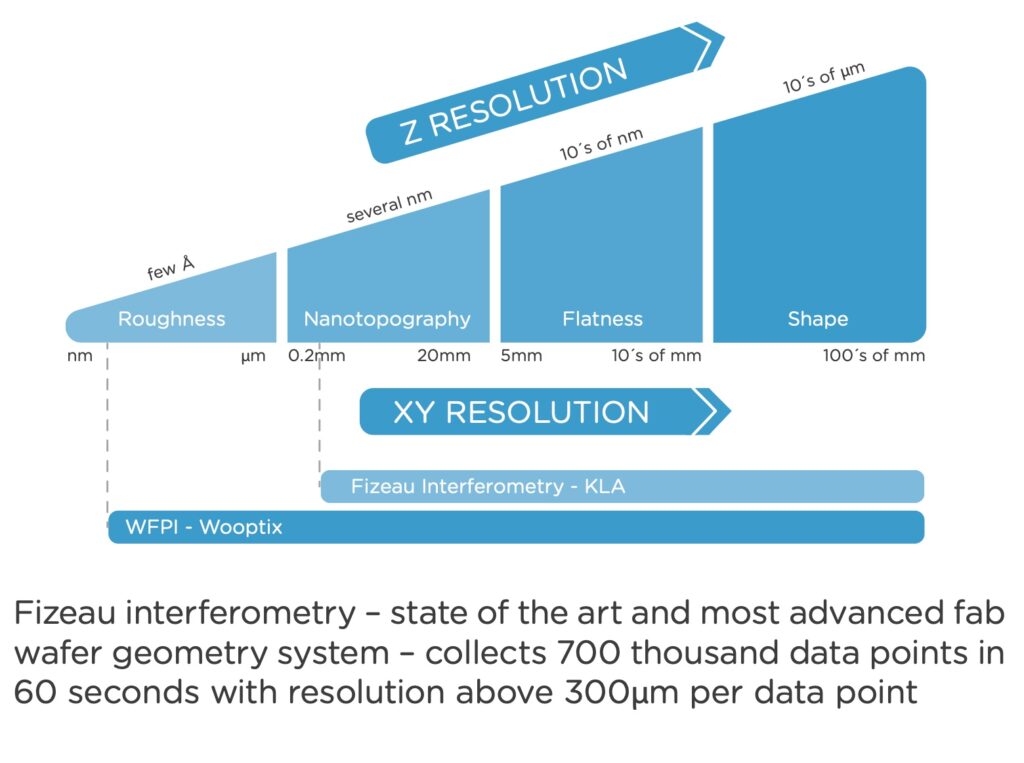
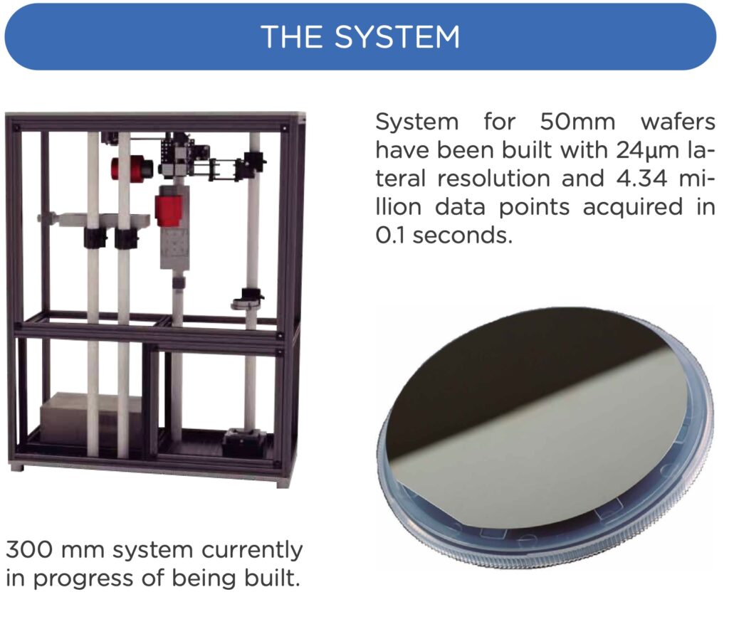
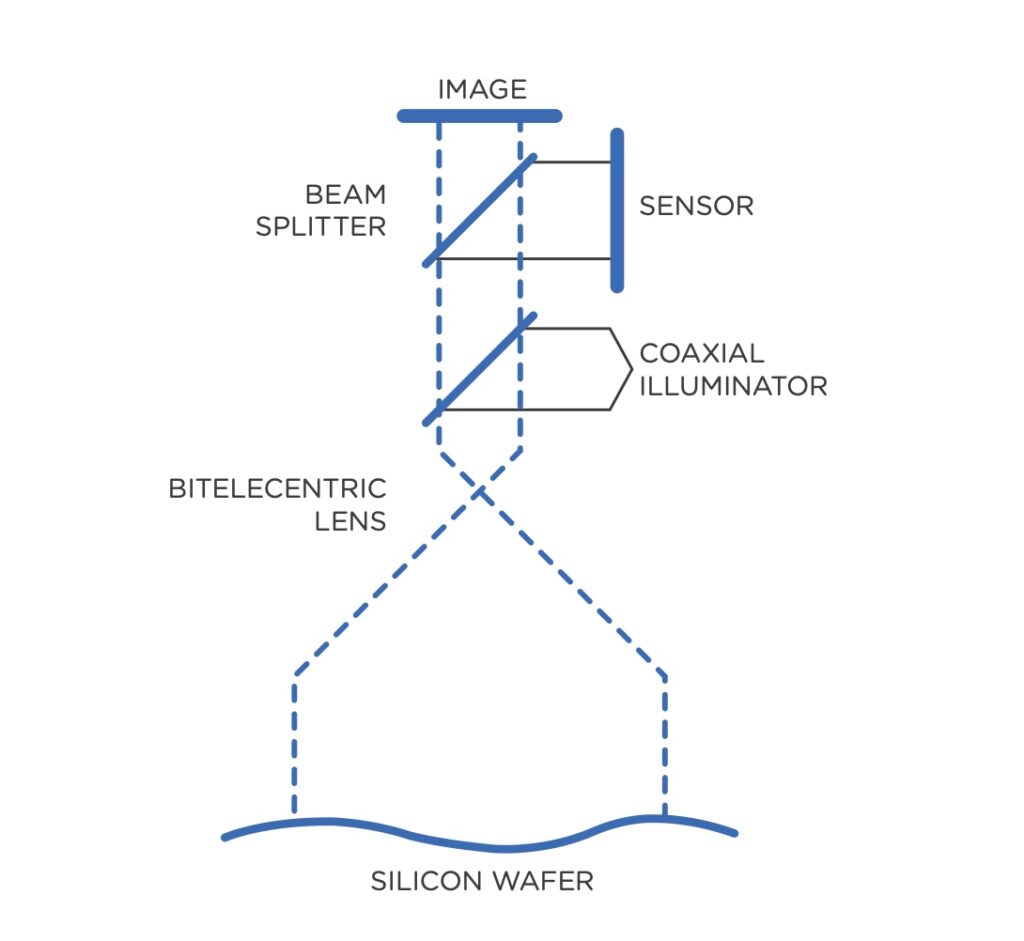
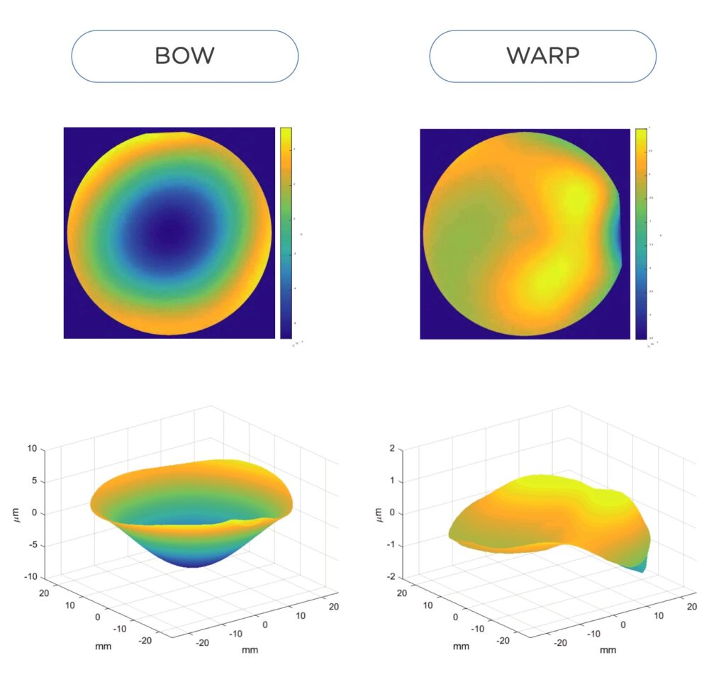
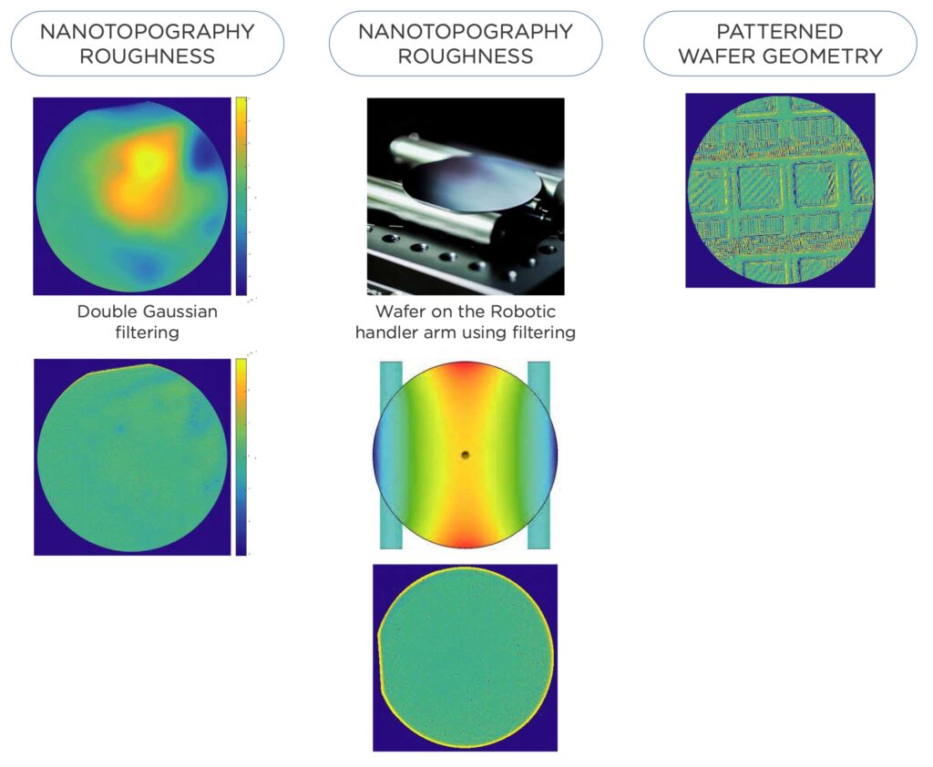
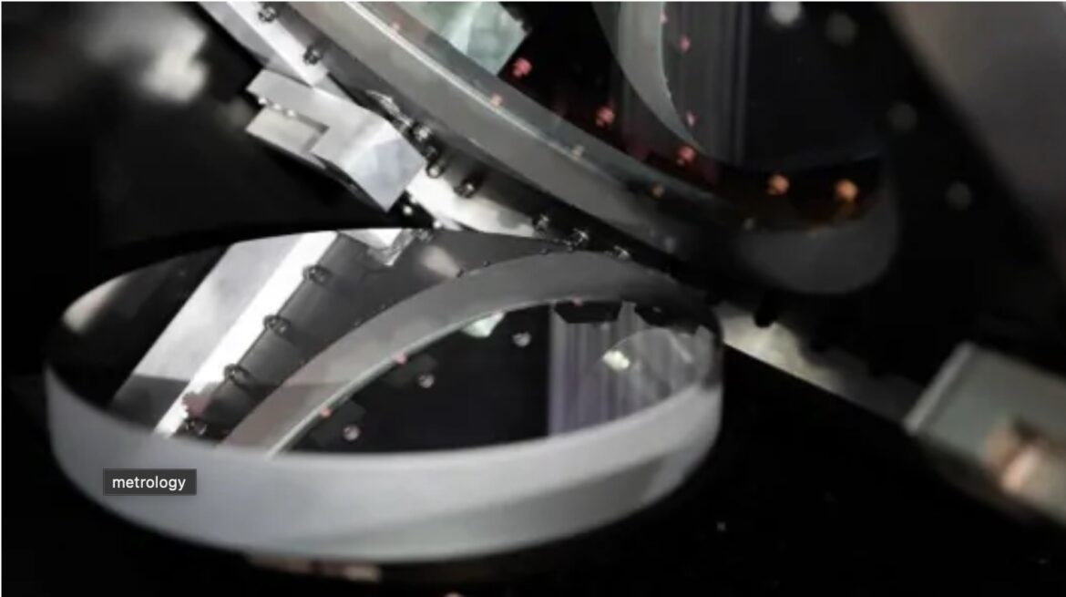
Wooptix, a Spanish company dedicated to the development of new imaging solutions, has introduced the Phemet® Laboratory System, a 300mm blank silicon wafer geometry metrology system that collects millions of topographic data points on a complete wafer in about few seconds. Headquartered in La Laguna, Tenerife, Canary Islands, Spain, the company builds on decades of optical research carried out at the astrophysics department of the University of La Lagune together with the Teide Observatory in Tenerife, one of the leading astronomical research centers Most important in the world. Series A funding in 2016 from ventures including Intel Capital has enabled the company to develop Phemet and bring it to commercialization for the semiconductor lab market. Phemet is based on a new technology for measuring wavefront phase that is unrelated to laser interferometry, currently the standard for measuring variations in shape and thickness of silicon wafers. Using Wooptix Wave Front Phase Imaging (WFPI), the single-camera Phemet lab version collects 7.6 million data points on a 300mm wafer in just 5 seconds with a lateral resolution of less than 100 µm and a noise level enabling topography detection of 0.3nm giving high resolution shape and form. thickness variation maps. By upgrading to a dual camera setup, the same number of pixels and noise level can be acquired in just 0.1 seconds, enabling high-speed manufacturing operations.
