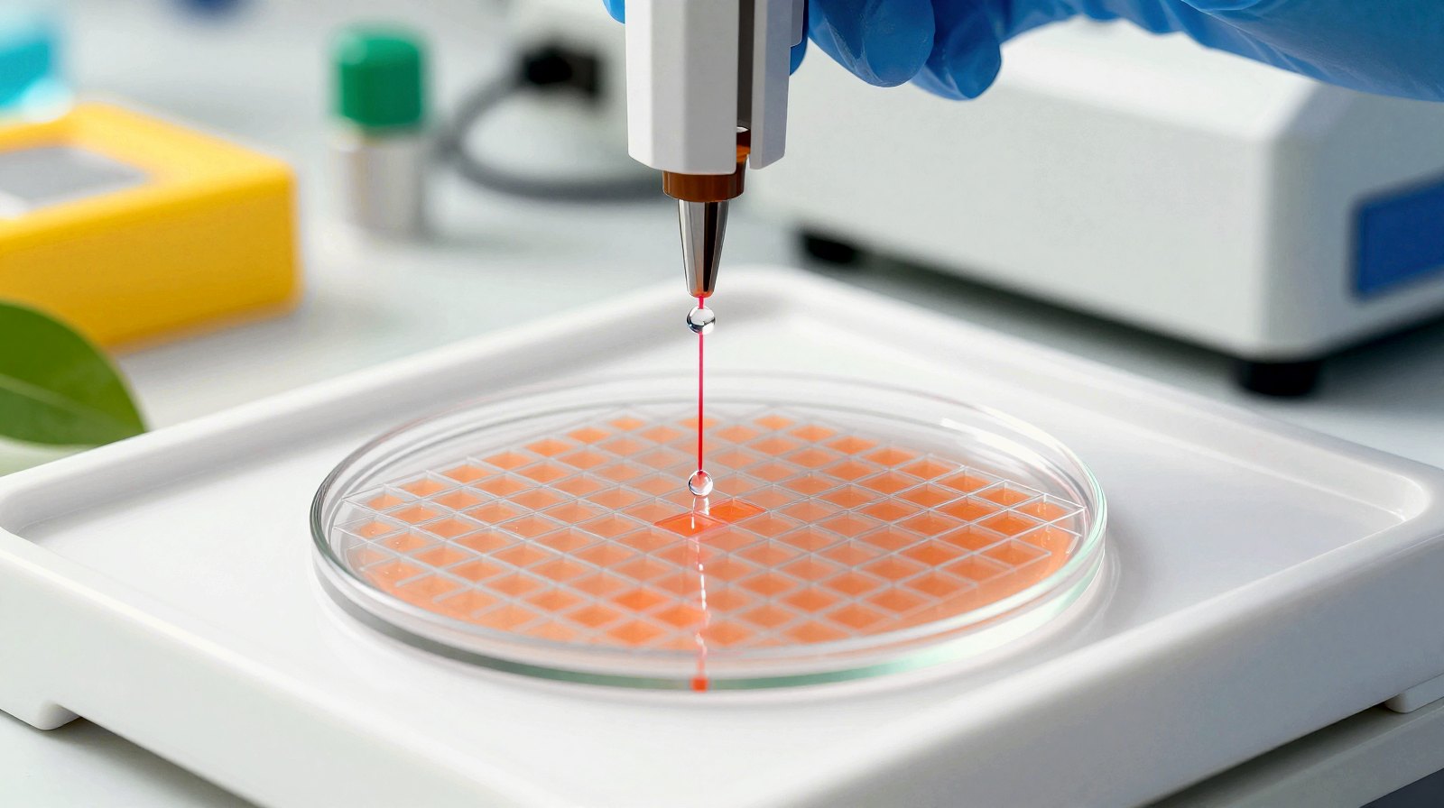
Japanese researchers have found a way to print the heart of a tiny atomic clock with an inkjet, much like printing a photo, and to tune it for each chip on a silicon wafer. The platform, announced on 19 November 2026 by Japan’s National Institute of Information and Communications Technology (NICT) and four partners, should make chip-sized atomic clocks faster to design.
Why it matters: your phone, the mobile network and many cars rely on satellite navigation signals (GNSS, the family that includes GPS and Galileo) to know the exact time. When that signal is lost or jammed, a small atomic clock on a chip can keep time instead. Making those clocks easier to build and optimise could put precise backup timing into many more devices.
What is a chip-scale atomic clock?
An ordinary quartz clock counts the vibrations of a tiny crystal, which drift with temperature and age. An atomic clock counts something that never changes: the natural “tick” of atoms. In a chip-scale clock, a laser shines through a minute glass cell filled with rubidium vapour, and electronics lock onto the atoms’ signal.
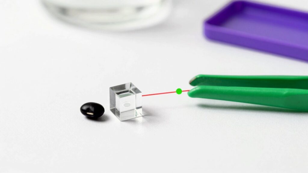
The trick is called coherent population trapping (CPT). When two laser beams hit the rubidium atoms at exactly the right frequencies, the atoms suddenly stop absorbing light and the cell becomes see-through. That “dark state” happens in a very narrow band, so it makes an extremely precise reference. NICT’s release shows one of these cells next to a black soybean for scale.
The problem: getting the gas just right
Besides rubidium, each cell holds a small amount of nitrogen gas. Nitrogen calms the rubidium atoms down, and the amount of it strongly affects how good the clock is. Until now, according to NICT, the gas pressure inside a cell could only be checked after the cell was finished, which makes optimising a design slow trial and error.
How the inkjet method works
The team uses rubidium azide (RbN3), a solid that breaks down into rubidium atoms and nitrogen gas when heated. Here is the process described by NICT:
- A custom inkjet printer deposits tiny particles of rubidium azide onto glass wafers with high precision.
- A silicon layer with etched cavities is bonded between two glass wafers, so laser light can pass through each cavity.
- Heat breaks the rubidium azide down inside the sealed cells, releasing rubidium vapour and nitrogen.
- The wafer is cut into individual chips, the same way computer chips are made.
The key result: the more rubidium azide the printer drops in, the more nitrogen ends up in the cell, in a strongly linear way. That means the gas pressure can be dialled in when the cell is printed. Cells with different amounts can be made side by side on the same wafer and compared, instead of building one batch after another.
What they measured
Using CPT measurements, the researchers worked out which nitrogen pressures give the best clock performance, and showed those conditions can be optimised systematically in a wafer-level process. The study, “Nitrogen-Pressure Dependence of Coherent Population Trapping Signal Characteristics in Microfabricated Rubidium Vapor Cells”, is published in the IEEE Open Journal of Ultrasonics, Ferroelectrics, and Frequency Control. Because the signal from such a small cell is very weak, the team also built a packaged measurement system to read it.
The work is a joint effort: NICT led and coordinated it, Kyoto University designed and made the cells, Tokyo Metropolitan University analysed the atomic signals, TOYOBO MC made the rubidium azide and the patterning method, and NEOARK built the measurement systems, according to the release on EurekAlert.
What the release does not give: the optimum pressure values, cell sizes, the number of cells per wafer or a finished clock’s stability. It is a manufacturing and design platform, not a finished product.
What it means for you
You will not buy an “inkjet atomic clock”. But the places NICT lists for chip-scale clocks touch everyday life: backup timing when satellite signals fail, time synchronisation in communication networks, equipment on satellites, autonomous vehicles and sensor systems. Cheaper, better clocks in those systems mean networks and navigation that cope better when GNSS is jammed or unavailable.
What happens next
The team plans to use the platform to optimise cell structures and fabrication conditions further, aiming at high-performance cells for the next generation of chip-scale atomic clocks. The project is funded by Japan’s Ministry of Internal Affairs and Communications as part of research into high-precision time synchronisation.
Read next
- Beyond EUV: nanoimprint and the new technologies breaking frontiers for next-gen silicon
- Record 7 eV semiconductor becomes a working transistor
- What are the CPU, GPU, NPU and TPU? The definitive guide
The week's best tech stories, free
One email a week with the stories that matter, explained simply. No spam.
Sources
- NICT: New MEMS Atomic Cell Platform Accelerates Design Optimization for Chip-Scale Atomic Clocks (19 Nov 2026)
- EurekAlert!: the NICT release (19 Nov 2026)
- IEEE Open Journal of Ultrasonics, Ferroelectrics, and Frequency Control: the research paper (DOI 10.1109/OJUFFC.2026.3739231)