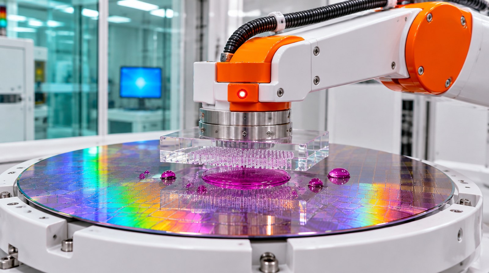
Almost every top chip in the world is printed with one kind of machine: an EUV scanner from the Dutch company ASML. Japan wants to offer other routes. Canon now sells a chip “printer” that works like a rubber stamp, Dai Nippon Printing has made stamps fine enough for future 1.4-nanometre chips, Nikon is building mask-free printers for chiplets, and a lab in Okinawa has sketched a much simpler EUV machine.
Why it matters: lithography, the step that “prints” circuit patterns onto silicon, is the most expensive part of making advanced chips. Cheaper or thriftier ways to do it could help more countries, labs and companies build modern chips, and cut the huge electricity bill of chip factories. None of these ideas has replaced EUV yet, so here is what is real, what is promised and what is still missing.
Key takeaways
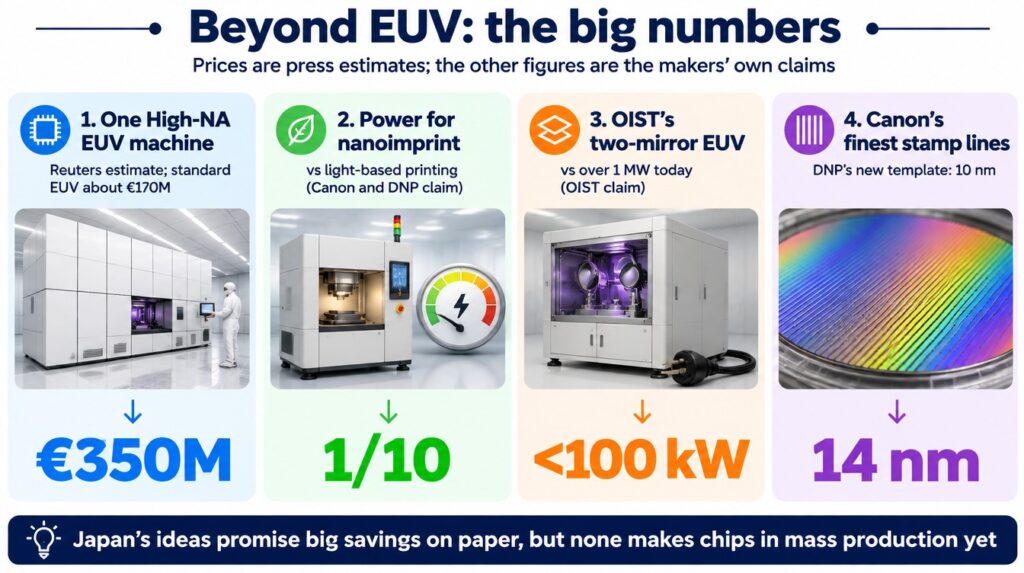
- EUV rules the top end: only ASML makes EUV machines, at about €170 million to €350 million each (press estimates).
- Canon’s stamp is real: its FPA-1200NZ2C nanoimprint machine prints 14 nm lines (5 nm-class chips) and shipped to a US research consortium in Texas in 2024.
- Finer stamps are coming: Dai Nippon Printing (DNP) showed a 10 nm template for 1.4 nm-generation chips and plans mass production in 2027.
- Big energy claims: Canon and DNP say nanoimprint uses about a tenth of the power; OIST says its EUV design needs under 100 kW instead of over 1 MW (makers’ own figures).
- New transistors too: 2 nm-class chips now wrap the gate all around the channel, and power wires are moving to the back of the chip.
- Not in mass production yet: defects, layer alignment and stamp lifetime are still the hurdles, and memory chips are the most likely first users.
First, what is EUV, and why look beyond it?
Making a chip is a bit like making a photo print, over and over. A wafer (a thin disc of silicon) is coated with a resist, a light-sensitive layer like the coating on old camera film. Light shines through a mask, a stencil with the circuit drawing, and “draws” the pattern onto the resist. Repeat for dozens of layers and you get billions of transistors (the tiny on-off switches that do the computing).
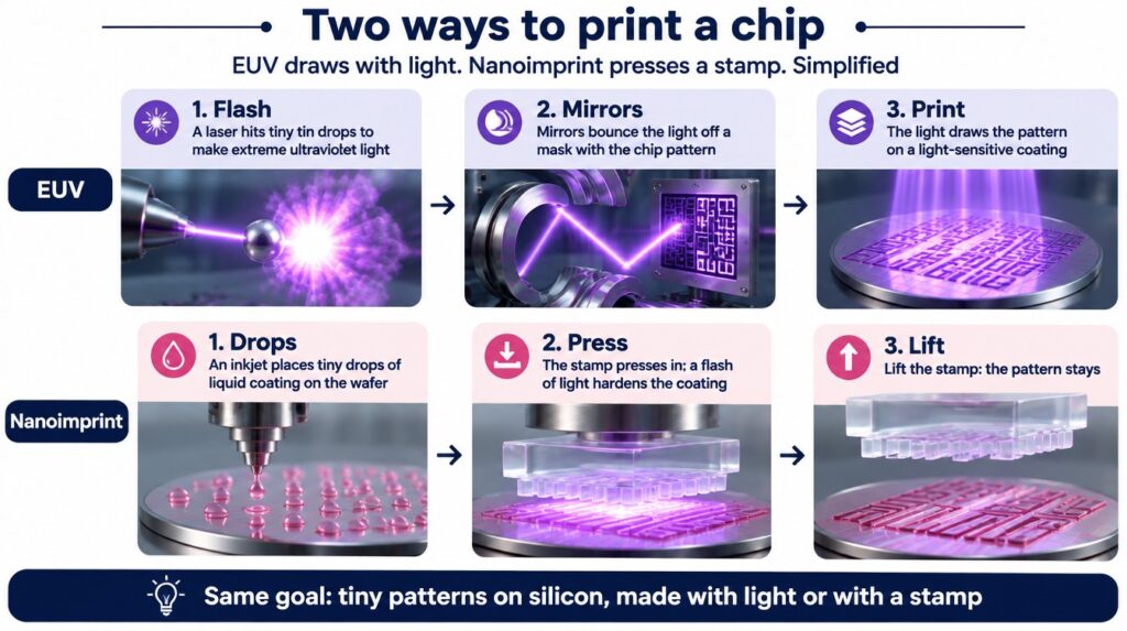
The smaller the drawing, the shorter the light you need, just as a fine pencil draws thinner lines than a fat marker. EUV (extreme ultraviolet) light has a wavelength of only 13.5 nm, close to X-rays. To make it, a laser first flattens tiny falling drops of molten tin, then a second pulse turns each one into a glowing plasma, 50,000 times a second, ASML explains. Even air absorbs that light, so the whole trip happens in a vacuum and is steered by mirrors instead of lenses, ASML adds.
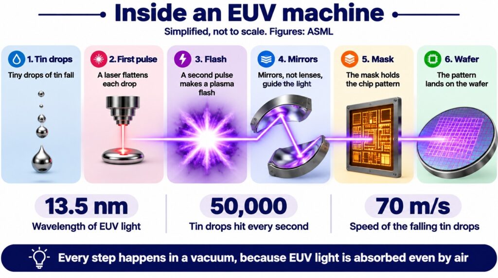
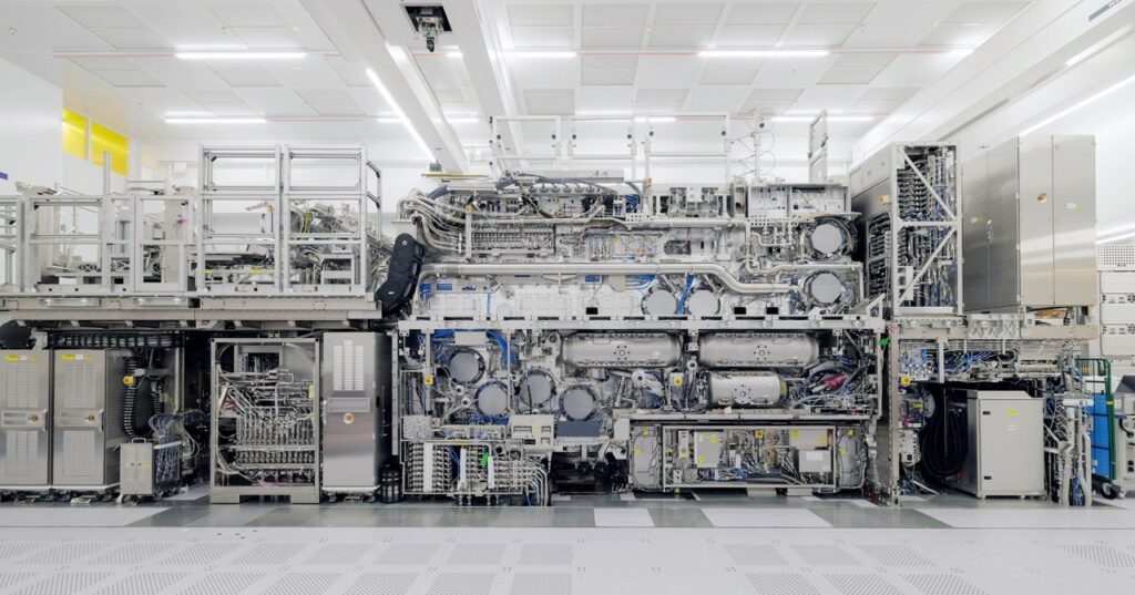
It works brilliantly, but it is a giant. Reuters put the newest High-NA EUV machine at about €350 million each, as ThePrint carried it, while standard EUV costs around €170 million, Tom’s Hardware reports. And only ASML sells them. That is the gap Japan’s engineers are aiming at.
Why smaller chips need new transistors
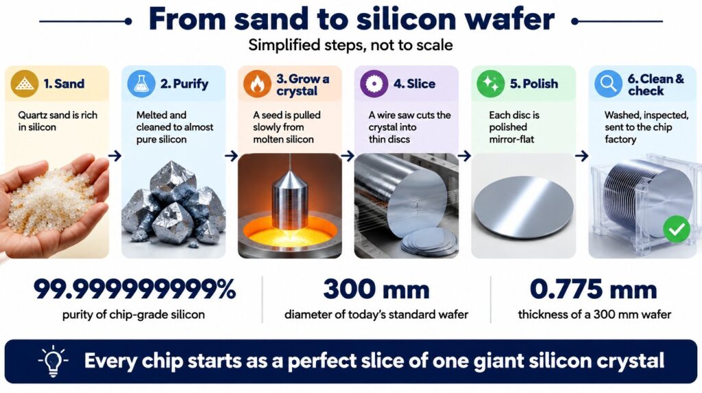
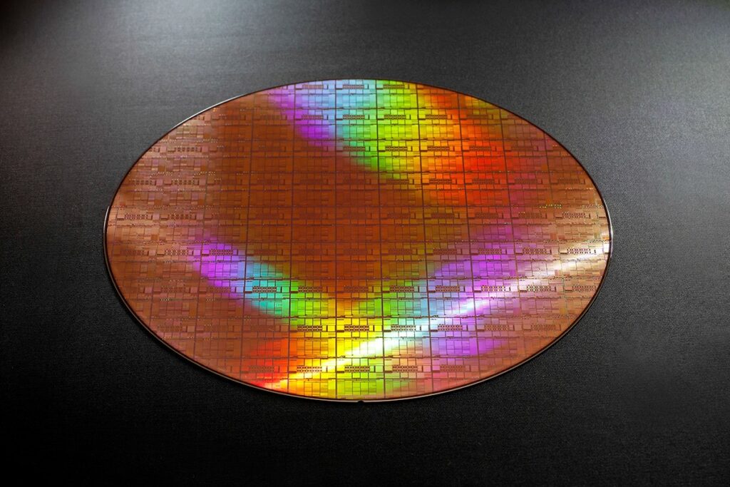
Every chip starts as a wafer: a thin, mirror-polished slice cut from one huge crystal of almost perfectly pure silicon. Here is how sand becomes that slice.
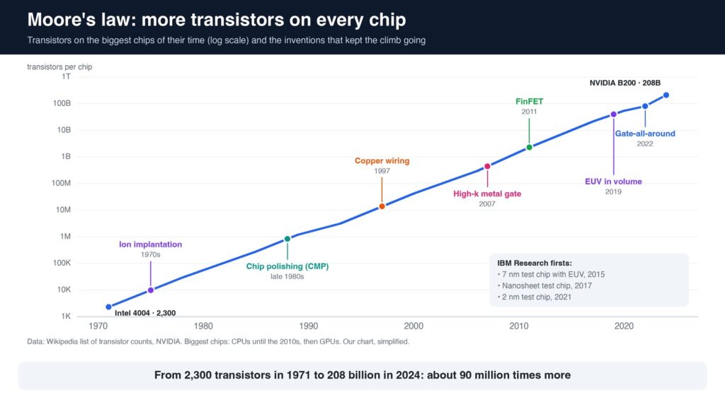
All of this keeps alive an idea from 1965: Intel co-founder Gordon Moore’s observation that the number of transistors on a chip doubles roughly every two years, now known as Moore’s law (Wikipedia). The biggest chips went from 2,300 transistors in 1971 to 208 billion in NVIDIA’s B200 in 2024 (transistor count list, NVIDIA), and every big step needed a new invention.
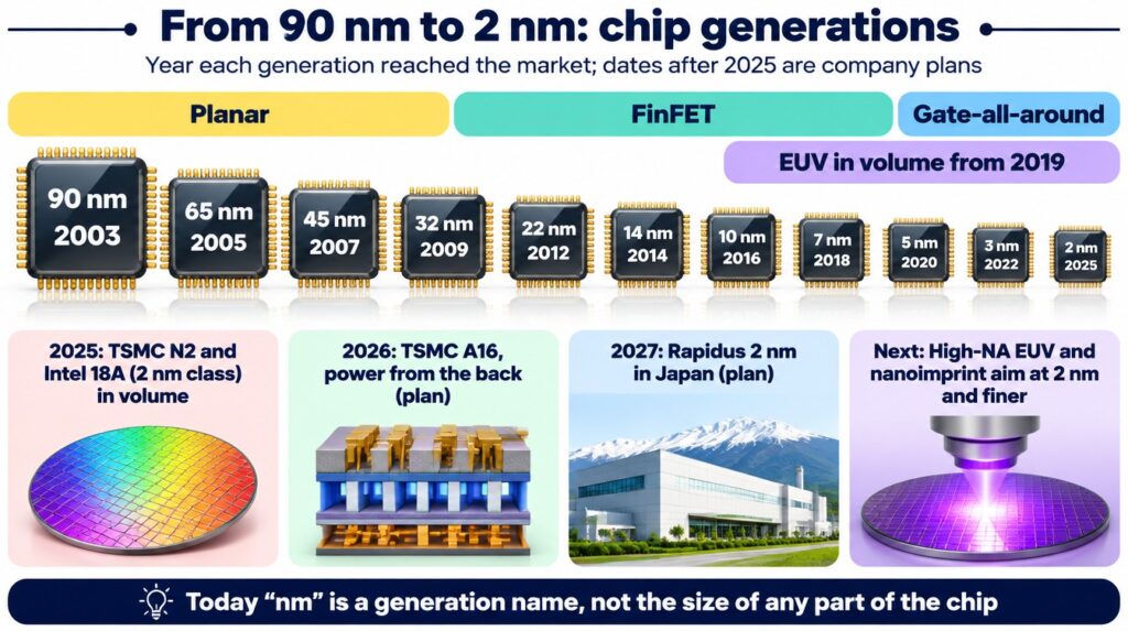
First, a surprise: today’s “2 nm” or “3 nm” names are generation labels, not the size of any real part of the chip. They stopped matching a single measurement years ago, as IEEE Spectrum explains and an IEEE Spectrum proposal for a better yardstick also argues. What keeps shrinking is how many transistors fit in the same space.
To keep packing them in, the switch itself had to change. Picture a transistor as a tap on a garden hose: the gate squeezes the channel to stop or let current flow. Old “planar” transistors pressed on the channel from the top only. In 2011 Intel announced 3-D “tri-gate” transistors, better known as FinFETs, for its 22 nm chips, gripping a raised fin on three sides, as ScienceDaily and AnandTech reported.
The newest step is gate-all-around (GAA): the channel becomes a stack of thin sheets, and the gate wraps around every one, so less current leaks when the switch is off, IEEE Spectrum and Semiconductor Engineering explain. Samsung started making 3 nm GAA chips in June 2022, according to Samsung and AnandTech. TSMC’s N2, its first GAA process, entered volume production in the fourth quarter of 2025, Tom’s Hardware and TechSpot report, and Rapidus showed its first working 2 nm GAA prototypes in July 2025, as Rapidus and Tom’s Hardware reported.
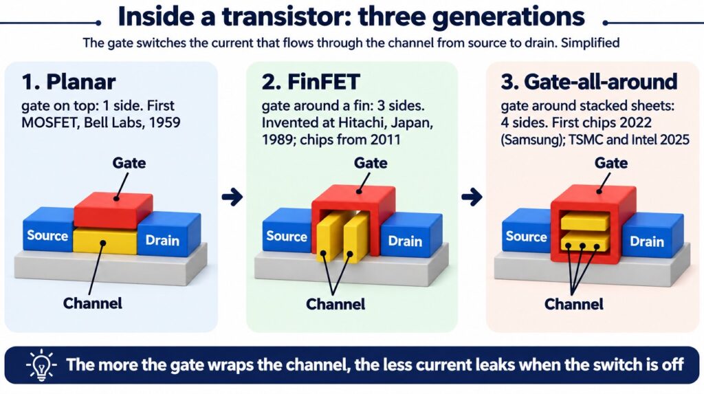
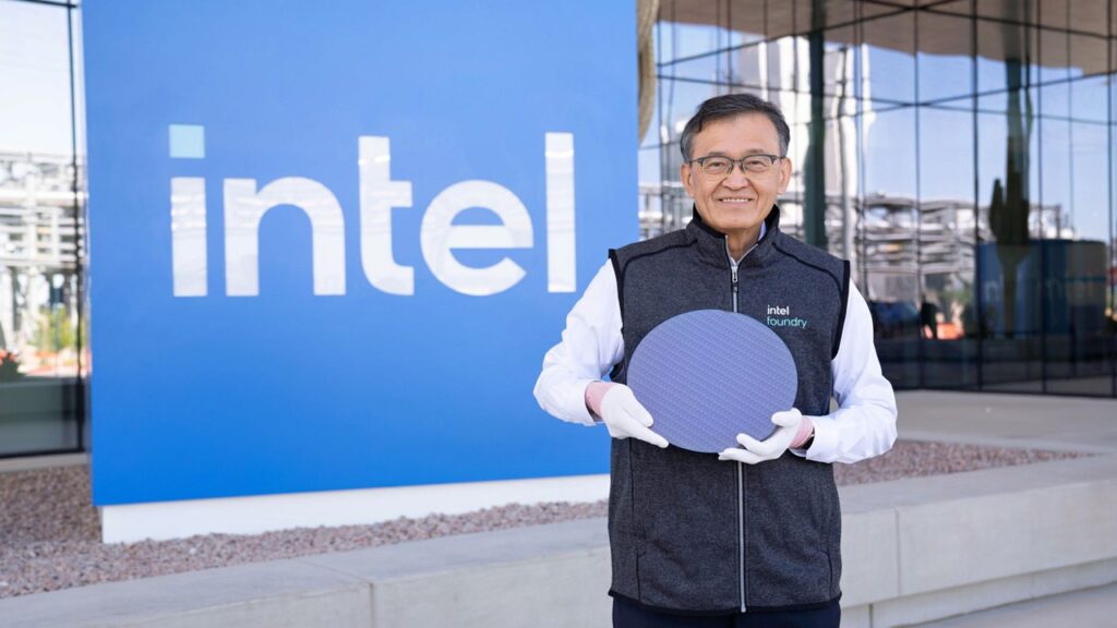
The other trick is backside power: moving the power wires underneath the transistors, a bit like putting a building’s water pipes in the basement so every floor has more room. Intel’s 18A, which it calls its first “2-nanometre class” node, combines GAA transistors (RibbonFET) with backside power (PowerVia) in its Panther Lake laptop chips, according to Intel and eeNews Europe. TSMC plans its own version, A16, for the second half of 2026, AnandTech and Semiconductor Engineering reported.
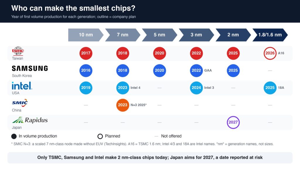
So who can actually make these newest chips? Only a handful of companies. Samsung started making its first 2 nm phone chip, the Exynos 2600, in 2025, TrendForce reported, joining TSMC and Intel. China’s SMIC, without EUV, has pushed its 7 nm-class process further but remains well short of real 5 nm, according to TechInsights, Tom’s Hardware and Mark LaPedus. Rapidus still targets the second half of its fiscal year 2027, but Bloomberg reported on 10 November 2026 that it is likely to miss that date after trouble making working 2 nm SRAM memory; Rapidus says it is on track, Electronics Weekly adds.
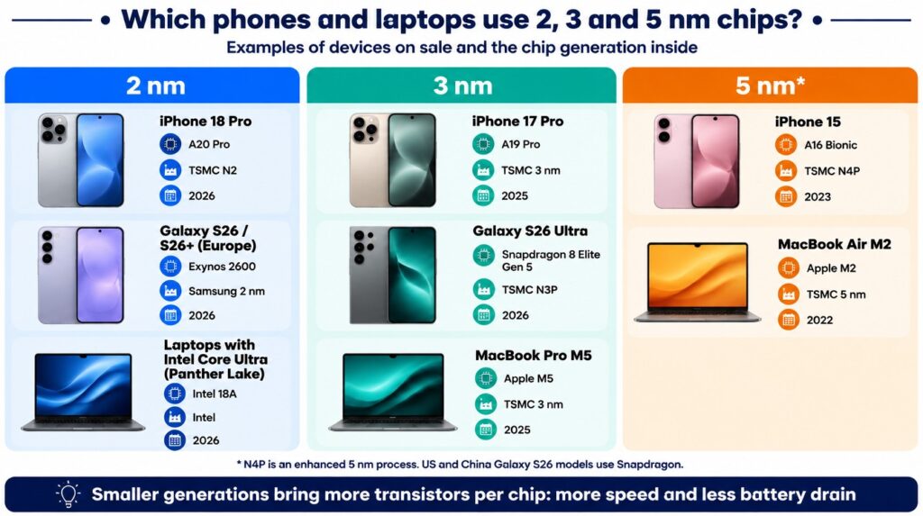
You probably carry one of these generations in your pocket. Here are some phones and laptops on sale and the chip generation inside each one (MacRumors, Android Authority, TechNode, Yole).
Nanoimprint: printing chips like a rubber stamp
Canon’s idea skips the light show. In nanoimprint lithography (NIL) a mask carved with the circuit pattern is pressed straight into the resist on the wafer, “like a stamp”, Canon says. Think of a waffle iron: the pattern is in the plate, and pressing it into the batter copies every square at once. Because no lenses or mirrors sit in between, the tiny features on the mask are copied faithfully.
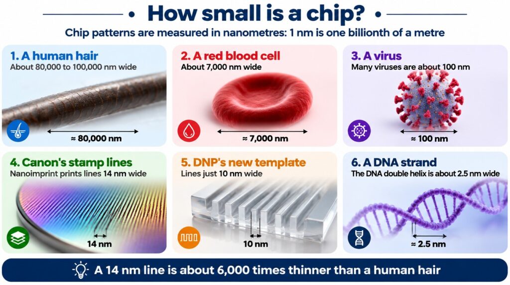
Canon launched its FPA-1200NZ2C in October 2023. It prints lines just 14 nm wide, which Canon says is equal to the 5 nm node (a “node” is a chip generation name rather than a ruler measurement). With better masks, Canon expects 10 nm lines, matching the 2 nm generation used in today’s most advanced phone and AI chips.
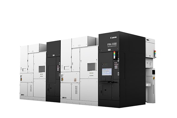
On 26 September 2024 Canon shipped one to the Texas Institute for Electronics, a consortium backed by the University of Texas at Austin, for research and prototype chips, according to Canon’s release and The Register. Canon’s CEO Fujio Mitarai has said its price will have “one digit less” than ASML’s EUV, as Tom’s Hardware reported from a Bloomberg interview, though no list price is public.
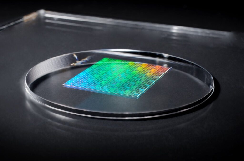
A stamp is only as good as its pattern, and that is where another Japanese giant comes in. In December 2025 Dai Nippon Printing (DNP) showed a nanoimprint template with 10 nm lines, aimed at 1.4 nm-generation logic chips. It got there with a trick called double patterning, which splits one dense drawing into two easier ones. DNP says the template can replace part of the EUV steps, uses about one-tenth of the exposure power of today’s methods, and should reach mass production in 2027, according to DNP and Bits&Chips.
What nanoimprint can’t do yet
Touching the wafer is NIL’s superpower and its weak spot. A single speck of dust trapped between stamp and wafer can spoil a chip or even damage the mask, Canon’s engineers explain in a company interview. Every layer must also sit on the one below with nanometre precision (engineers call it overlay), and any flaw in the stamp is copied onto every chip, Semiconductor Engineering noted.
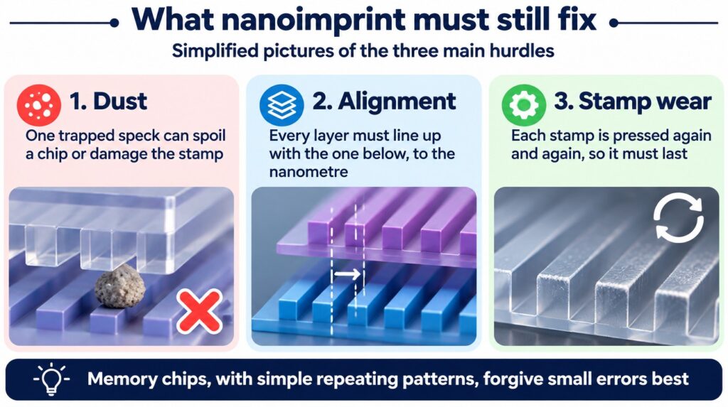
That is why no contract chipmaker has yet committed to NIL for high-volume production, Tom’s Hardware points out. Memory looks like the most likely first home: memory chips repeat the same simple pattern millions of times, which forgives small errors better. Japan’s memory maker Kioxia (formerly Toshiba Memory) has tested Canon’s machines for 3D NAND, the chips inside SSDs, for years, Asia Times reported, but has not announced mass production with it.
The stamp idea is already branching out. In January 2026 Canon unveiled inkjet-based adaptive planarization: an inkjet places just the right amount of liquid where the wafer has dips, then a flat glass plate presses it level, leaving bumps of 5 nm or less across a whole 300 mm wafer in one go. Canon aims to sell the equipment in 2027, according to Canon and MONOist.
A simpler, thriftier EUV: two mirrors instead of six
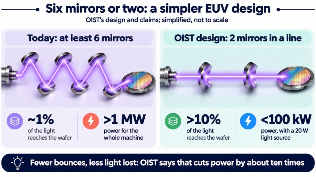
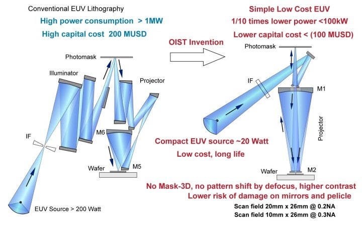
Instead of replacing EUV, a team at the Okinawa Institute of Science and Technology (OIST) led by Professor Tsumoru Shintake wants to shrink it. Today’s EUV projector bounces light off at least six mirrors, and only about 1% of the light reaches the wafer. Their design uses just two mirrors in a straight line, like a telescope, so more than 10% gets through, OIST says.
The result, on paper: a 20-watt light source and a whole machine using under 100 kW, against more than 1 MW for current systems, as DCD also reports. OIST has filed a patent, but it is unclear how close the design is to a working commercial tool, Tom’s Hardware notes.
The quiet giants: light, chemicals and chiplet printers
Even in factories full of ASML machines, Japanese parts and chemicals are everywhere.
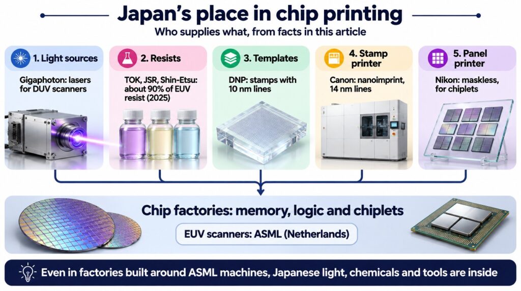
- Light sources: Gigaphoton, a Komatsu company in Tochigi, makes excimer lasers, the light sources inside the deep-ultraviolet (DUV) scanners that work alongside EUV in chip factories,, optics.org reported.
- Resists: three Japanese firms, Tokyo Ohka Kogyo (TOK), JSR and Shin-Etsu Chemical, supplied about 90% of the world’s EUV resist in 2025, according to QYResearch figures cited by Digital Today. Japanese makers held 72.5% of all photoresist in 2021, SCMP adds.
- Metal-oxide resists: for High-NA EUV, resists built from tiny metal-oxide clusters, rather than plastic-like molecules, can soak up more of the scarce EUV light, which helps print sharper, smaller features. In September 2025 JSR’s US unit Inpria and Lam Research agreed to develop them together for High-NA patterning, JSR announced; I-Connect007 covered it too.
- Chiplet printers: a chiplet is like building a computer from LEGO bricks instead of one carved block, and the bricks are wired together on big panels. Nikon’s DSP-100 prints those wires with no mask at all,: 1 micrometre lines on panels up to 600 mm square, with first deliveries planned in Nikon’s fiscal year 2026, Nikon says. A faster successor is due in fiscal 2027, TrendForce reports.
More Japanese breakthroughs for next-gen chips
Printing is only one step. Japanese companies are pushing the rest of the chip-making line too:
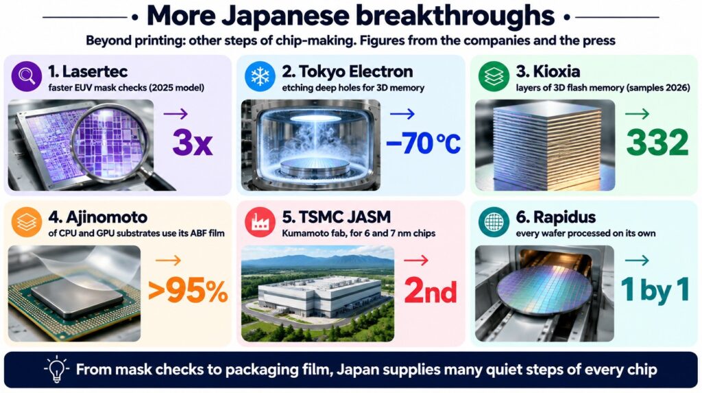
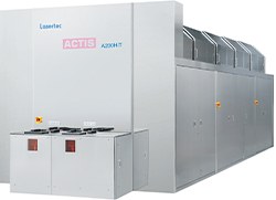
- Checking the masks: an EUV mask must be flawless, and the surest check uses EUV light itself (“actinic” inspection). Lasertec launched the first such machine in 2019 and, in October 2025, a model that inspects three times faster, according to Lasertec and Dempa.
- Ice-cold etching: Tokyo Electron’s etcher works at about −70 °C and digs holes 10 micrometres deep in 33 minutes for 3D memory with more than 400 layers, Tom’s Hardware reported; TheElec said shipments would start in 2025.
- Taller memory towers: Kioxia began sampling 332-layer 3D flash memory in July 2026, built on two separate wafers (control circuits and memory cells) bonded face to face, a method it calls CBA, say Kioxia and Blocks and Files.
- The film inside big chips: Ajinomoto, the food company famous for MSG seasoning, makes the insulating film (ABF) used in more than 95% of CPU and GPU package substrates, and plans to invest at least ¥25 billion by 2030 to make 50% more, TrendForce and TechRadar report.
- New factories: TSMC’s Japanese venture JASM runs a fab in Kumamoto and has started building a second one for 6 and 7 nm chips, according to TSMC and TechNode. In Hokkaido, Rapidus processes every wafer one at a time instead of in batches, collecting data to help AI improve its yields, as Rapidus and Tom’s Hardware reported.
Where the rest of the world fits
Europe owns the top end through ASML in the Netherlands. South Korea is racing ahead with it: SK hynix assembled the first High-NA EUV machine for mass production at its Icheon fab in September 2025, Tom’s Hardware and TrendForce report, and Samsung has its own. Taiwan‘s TSMC, the biggest contract chipmaker, builds its leading chips with EUV, and JSR is building its first photoresist plant in Taiwan, Taiwan News and Tom’s Hardware report.
China, which cannot buy EUV machines under export rules, is chasing nanoimprint too: local firm Prinano delivered its first step-and-repeat NIL tool in 2025, Notebookcheck reported. And Japan’s own leading-edge hope, Rapidus and its 2 nm factory in Hokkaido, prints with ASML’s EUV. For Latin America, Spain and the rest of the EU, DNP’s pitch is the interesting part: cheaper patterning for chipmakers without EUV.
What happens next
- 2026-2027: Nikon’s first DSP-100 deliveries for chiplet packaging (its fiscal year ends in March 2027).
- 2027: DNP’s mass production of 10 nm nanoimprint templates and Canon’s first planarization machines, if plans hold.
- The big one: a memory or logic maker announcing nanoimprint for real mass production. Kioxia is the name to watch.
- Okinawa: any prototype or industry partner for OIST’s two-mirror EUV would be the first sign it can leave the lab.
EUV is not going anywhere soon. But the next chip in your phone may well carry a Japanese stamp, a Japanese resist or a Japanese laser somewhere inside.
Read next
- Rapidus 2nm: Japan’s bid to build the world’s tiniest chips
- Record 7 eV semiconductor becomes a working transistor
- What are the CPU, GPU, NPU and TPU? The definitive guide
The week's best tech stories, free
One email a week with the stories that matter, explained simply. No spam.
Sources
- Canon launches nanoimprint lithography system FPA-1200NZ2C – Canon, 13 October 2023
- Canon delivers FPA-1200NZ2C to the Texas Institute for Electronics – Canon, 26 September 2024
- Canon ships nanoimprint lithography machine – The Register, 1 October 2024
- Canon’s nanoimprint litho tool could disrupt wafer fab equipment market – Tom’s Hardware, November 2023
- Nanoimprint lithography (engineer interview) – Canon
- Canon achieves world first with inkjet-based wafer planarization – Canon, 13 January 2026
- Canon inkjet planarization report – MONOist (ITmedia), January 2026
- DNP achieves 10nm line-pattern resolution on nanoimprint template – Dai Nippon Printing, 9 December 2025
- DNP unveils 10 nm nanoimprint template – Bits&Chips, 10 December 2025
- Japan’s DNP targets 2027 mass production of 1.4nm nanoimprint templates – Tom’s Hardware, 2025
- What happened to nanoimprint litho? – Semiconductor Engineering, 29 March 2018
- EUV lithography systems – ASML
- ASML ships second High NA EUV machine – Reuters via ThePrint, April 2024
- ASML’s High-NA tool will cost $380 million – Tom’s Hardware, 2024
- Innovative EUV lithography technology dramatically increases energy efficiency – OIST, 29 July 2024
- Japanese scientists develop cheaper and more energy-efficient EUV lithography – DCD, 2024
- Japanese scientists develop simplified EUV scanner – Tom’s Hardware, 2024
- Company profile – Gigaphoton
- Komatsu to take full control of Gigaphoton – optics.org, 26 April 2011
- Japan’s materials grip strengthens in 2-nanometre era – Digital Today, 11 March 2026
- China targets Japan: what levers does Tokyo have? – South China Morning Post, January 2026
- JSR/Inpria and Lam Research enter cross-licensing and collaboration agreement – JSR, 16 September 2025
- JSR/Inpria, Lam Research enter cross licensing and collaboration agreement – I-Connect007, September 2025
- Orders begin for digital lithography system DSP-100 – Nikon, 16 July 2025
- Nikon targets panel packaging with new lithography system for FY27 – TrendForce, 9 June 2026
- Canon on cusp of nanoimprint chip-making revolution – Asia Times, November 2022
- JSR builds first Taiwan photoresist plant – Tom’s Hardware, May 2026
- JSR to build Taiwan plant to supply TSMC with photoresist – Taiwan News, 5 May 2026
- Canon launches FPA-8000iW – Silicon Semiconductor, 14 July 2020
- ASML and SK hynix assemble first commercial High-NA EUV system – Tom’s Hardware, September 2025
- SK hynix leads the pack with High-NA EUV for memory – TrendForce, 3 September 2025
- Prinano delivers first domestic nanoimprint lithography tool – Notebookcheck, 16 August 2025
- Light and lasers (how EUV light is made) – ASML
- 5 things you should know about High NA EUV lithography – ASML, 2024
- The status of Moore’s Law: it’s complicated – IEEE Spectrum
- A better way to measure progress in semiconductors – IEEE Spectrum (PDF copy), 2020
- Just how small is “nano”? – U.S. National Nanotechnology Initiative
- Semiconductor device fabrication (process node table) – Wikipedia, accessed 11 November 2026
- N7+ is first EUV process delivering customer products in high volume – TSMC, 7 October 2019
- Intel reinvents transistors using new 3-D structure – ScienceDaily, May 2011
- Intel announces first 22nm 3D Tri-Gate transistors – AnandTech, May 2011
- The nanosheet transistor is the next (and maybe last) step in Moore’s Law – IEEE Spectrum, 2019
- From FinFETs to gate-all-around – Semiconductor Engineering
- Samsung begins chip production using 3nm process technology with GAA architecture – Samsung, 30 June 2022
- Samsung starts 3nm production: the gate-all-around era begins – AnandTech, June 2022
- TSMC quietly begins volume production of 2nm-class chips – Tom’s Hardware, 2025
- TSMC’s 2nm N2 process officially enters volume production – TechSpot, 2025
- Rapidus achieves milestone with prototyping of 2nm GAA transistors – Rapidus, 18 July 2025
- Rapidus begins test production of 2nm circuits – Tom’s Hardware, July 2025
- Intel unveils Panther Lake architecture, first AI PC platform built on 18A – Intel, 9 October 2025
- Intel 18A anchors Intel’s Panther Lake and Xeon 6 platforms – eeNews Europe, October 2025
- TSMC’s 1.6nm technology announced for late 2026: A16 with Super Power Rail – AnandTech, April 2024
- TSMC uncorks A16 with Super Power Rail – Semiconductor Engineering, 2024
- Lasertec releases ACTIS A200HiT actinic EUV patterned mask inspection system – Lasertec, 31 October 2025
- Lasertec ACTIS A200HiT report – Dempa (AEI), 2025
- Chipmaking to go subzero: 3D flash made at -70C with next-gen tool – Tom’s Hardware, 2023
- Tokyo Electron cryogenic etcher shipments – TheElec, 2024
- Kioxia begins sample shipments of 10th-generation BiCS FLASH – Kioxia, 3 July 2026
- Kioxia sample shipping 332-layer 3D NAND – Blocks and Files, 3 July 2026
- Ajinomoto to invest JPY 25 billion by 2030 to expand ABF production – TrendForce, 1 April 2025
- Japanese firm behind MSG is ramping up production of key chip-packaging material – TechRadar, 2025
- JASM set to expand in Kumamoto, Japan – TSMC, 6 February 2024
- TSMC begins construction of Kumamoto second fab – TechNode, 28 October 2025
- Samsung reportedly starts Exynos 2600 mass production – TrendForce, 30 September 2025
- SMIC N+3 confirmed: Kirin 9030 analysis reveals how close SMIC is to 5nm – TechInsights, 11 December 2025
- Huawei Kirin 9030 made on SMIC N+3 but can’t compete with 5nm nodes – Tom’s Hardware, December 2025
- Can China make 5nm chips? – Mark LaPedus (Semiecosystem), 27 June 2025
- Japan’s Rapidus is said likely to miss mass production deadline – Bloomberg, 10 November 2026
- Delays reported at Rapidus – Electronics Weekly, 10 November 2026
- Intel unveils Panther Lake (newsroom) – Intel Newsroom, 9 October 2025
- 10 nm process – Wikipedia, accessed 11 November 2026
- 7 nm process – Wikipedia, accessed 11 November 2026
- 5 nm process – Wikipedia, accessed 11 November 2026
- 3 nm process – Wikipedia, accessed 11 November 2026
- 2 nm process – Wikipedia, accessed 11 November 2026
- Apple Unveils A20 Pro as First 2nm Smartphone Chip – MacRumors, 2026-09-09
- Apple announces A20 Pro chip with 2nm design – 9to5Mac, 2026-09-09
- Exynos 2600 is back in the Galaxy S26 – Android Authority, 2026
- The Exynos and Snapdragon split in the Galaxy S26 lineup – PhoneArena, 2026
- Exynos 2600 vs Snapdragon 8 Elite Gen 5 – Gizmochina, 2026-03-06
- Apple M5 series chips enter mass production with TSMC N3P – TechNode, 2025-02-07
- Apple A16 Bionic system-on-chip – Yole Group
- Wafer (electronics) – Wikipedia
- Moore’s law – Wikipedia
- Transistor count – Wikipedia
- NVIDIA Blackwell Platform Arrives (208 billion transistors) – NVIDIA, 2024-03-18
- IBM Unveils World’s First 2 Nanometer Chip Technology – IBM, 2021-05-06
- Fin field-effect transistor (Hitachi DELTA, 1989) – Wikipedia
- MOSFET (Bell Labs, 1959) – Wikipedia